
GRATIS

Cursos gratis (Auditar)


Inglés

Siempre Abierto

Guía de Registro en Coursera

Acerca de este curso
Compártelo


- Course Introduction
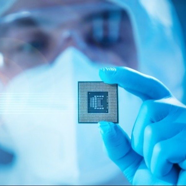
- Electron and ion beams are widely used for both qualitative and quantitative analysis of semiconductor materials and devices. They can be used to image structures with sub-nm resolution and to provide information about elemental composition and dopant concentration. This course describes the fundamentals of electron and ion beam characterization and includes a project that analyzes the surface roughness of a solar cell.
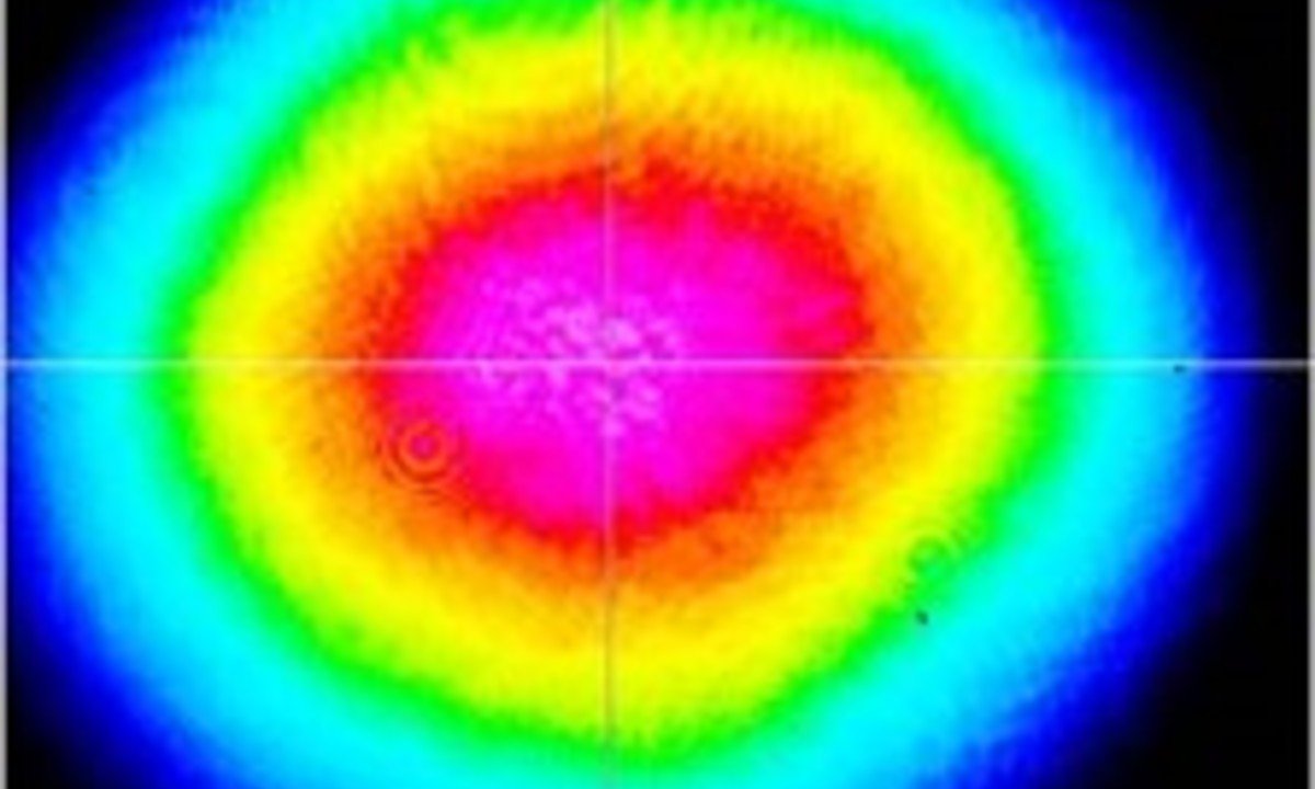
- Week 4.1: Scanning Electron Microscopy
- This week introduces the concepts of scanning electron microscopy and how it is used for both qualitative and quantitative sample analysis.
- Week 4.2: Auger Electron Spectroscopy
- This week, you will learn about Auger electron emission spectroscopy, a powerful technique for surface analysis.
- Week 4.3: Secondary Ion Mass Spectroscopy
- This week, you will learn about secondary ion mass spectroscopy and how it is used to measure the concentration and distribution of constituent materials in semiconductors.
- Week 4.4: Course Wrap-up and Project
- This week, you will complete a case study to assess your ability to use images obtained from an SEM for quantitative surface analysis.
Cursos relacionados

GRATIS Aprendiendo a aprender: Poderosas herramientas mentales…

Deep teaching solutions

Español
GRATIS Programación para todos (Introducción a Python)
University of Michigan
Inglés

GRATIS The Science of Well-Being
Yale
Inglés

GRATIS Negociación exitosa: Estrategias y habilidades esenciales
University of Michigan
Inglés

GRATIS Primeros Auxilios Psicológicos (PAP)
Universitat Autónoma de Barcelona
Español

GRATIS Chino para principiantes
Peking University
Inglés
¿Te apetece valorar
nuestra web?
4.3 / 5 ( 3432 votos )
¿Preparado para tu próximo proyecto laboral?
Copyright © 2022 Mooc. Todos los derechos reservados