
GRATIS

Cursos gratis (Auditar)


Inglés

Siempre Abierto

Guía de Registro en Coursera

Acerca de este curso
Compártelo


- Course Introduction
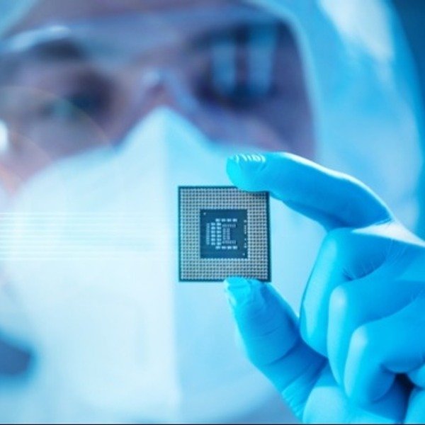
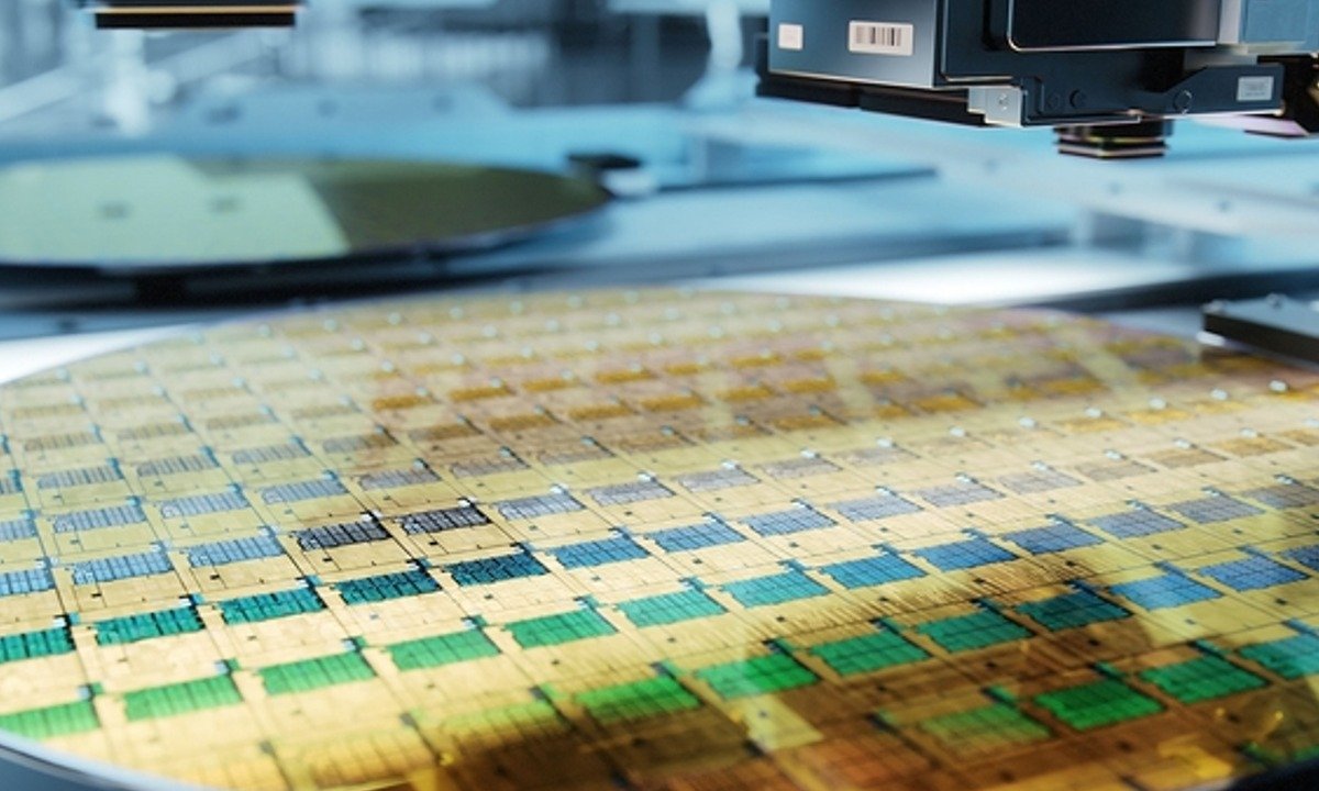
- Optical and X-ray techniques are powerful ways to characterize semiconductor thin films. They can be used to measure film thickness, purity and crystalline quality, and for compositional analysis. Modern techniques are fast, turn-key, and generally non-destructive, allowing for rapid assessment of material properties. This course describes the fundamentals of optical and X-ray characterization and provides real-world examples of how they are used in semiconductor manufacturing.
- Week 5.1: Reflectance Spectroscopy
- This week introduces the concept of reflectance spectroscopy: a rapid, convenient, and non-destructive technique for measuring the thickness of transparent materials.
- Week 5.2: Ellipsometry
- This week, you will learn about ellipsometry, a powerful technique that allows us to extract the thickness and refractive index of transparent layers as thin as a few nanometers.
- Week 5.3: Photoluminescence
- This week, you will learn about photoluminescence.
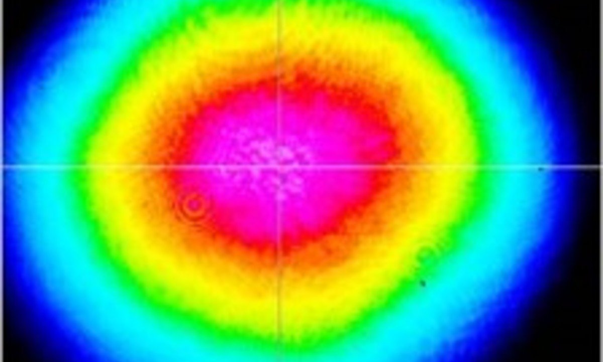
- Week 5.4: Electron Microprobe X-Ray Analysis
- This week, you will learn about electron microprobe X-ray analysis.
- Week 5.5: Course Wrap-up and Project
- This week, you will complete a case study to assess your ability to analyze electron microprobe x-ray images to determine the constituent elements in a 40 nm MOSFET.
Cursos relacionados

GRATIS Aprendiendo a aprender: Poderosas herramientas mentales…

Deep teaching solutions

Español
GRATIS Programación para todos (Introducción a Python)
University of Michigan
Inglés

GRATIS The Science of Well-Being
Yale
Inglés

GRATIS Negociación exitosa: Estrategias y habilidades esenciales
University of Michigan
Inglés

GRATIS Primeros Auxilios Psicológicos (PAP)
Universitat Autónoma de Barcelona
Español
GRATIS Chino para principiantes
Peking University
Inglés
¿Te apetece valorar
nuestra web?
4.3 / 5 ( 3432 votos )
¿Preparado para tu próximo proyecto laboral?
Copyright © 2022 Mooc. Todos los derechos reservados