
Impulsa tu carrera laboral
Cursos Gratis Online de las Mejores Universidades del Mundo

Más de 870 universidades ofertan Mooc:
¿Qué son los cursos Mooc?
Los Mooc son Cursos Online Gratis y Masivos. Aquí encontrarás más de 10K de todas las temáticas

Su potencial reside en su capacidad para conectar el conocimiento de los participantes.

Están siempre actualizados y orientados al mundo laboral.

Puedes realizarlos a tu ritmo, tienen una duración media 30/40 horas (5-7 semanas)

Una vez que los termines, puedes obtener un certificado
Cursos Mooc más populares
Encuentra el curso que impulsará tu carrera profesional
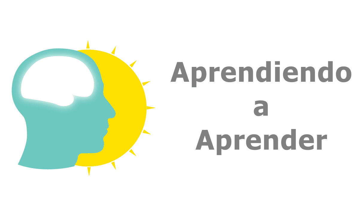


GRATIS Aprendiendo a aprender: Poderosas herramientas mentales…

Deep teaching solutions

Español
Estadísticas de los logros
obtenidos por los
estudiantes de Mooc.
*Fuente de datos: COURSERA.ORG
Consiguió un beneficio tangible en su carrera profesional
Consiguió un aumento de sueldo o ascenso
Qué dicen los usuarios sobre los Mooc
+ de 100M de estudiantes han realizado cursos Mooc


Excelente
Gran curso. Hubo muchos conceptos en este curso que me dieron una nueva perspectiva/herramienta para hacer mejor mi trabajo

Excelente
Muy buen curso, en contenido y en metodología, recomendable para todos aquellos que busquen mejor desempeño en sus actividades.

Excelente
In contrast with most courses, it’s not a sole effort. You need to engage with other students to do actual negotiations – something that makes the course more valuable and interesting

Excelente
Muy buen curso. Temas y situaciones de casos reales que ayudan mucho a la vida laboral

Excelente
Gran curso. Hubo muchos conceptos en este curso que me dieron una nueva perspectiva/herramienta para hacer mejor mi trabajo

Excelente
Muy buen curso, en contenido y en metodología, recomendable para todos aquellos que busquen mejor desempeño en sus actividades
Excelente
Gran curso. Hubo muchos conceptos en este curso que me dieron una nueva perspectiva/herramienta para hacer mejor mi trabajo

Excelente
Muy buen curso. Temas y situaciones de casos reales que ayudan mucho a la vida laboral
Excelente
Gran curso. Hubo muchos conceptos en este curso que me dieron una nueva perspectiva/herramienta para hacer mejor mi trabajo
Pertenece a esta gran red
Síguenos en nuestras redes sociales:
Últimas guías y artículos
Últimos post de nuestro blog


¿Te apetece valorar
nuestra web?
4.3 / 5 ( 3432 votos )
¿Preparado para tu próximo proyecto laboral?
Copyright © 2022 Mooc. Todos los derechos reservados